Introduction to Topological Insulators
Topological insulators represent a new quantum state of matter which are insulating in their bulk interior but metallic on the topologically protected edge or surface states [1- 3]. As the consequence of the topological order, the surface states cross the Fermi surface odd number of times and are guaranteed to be metallic. They also have a linear energy-momentum dispersion relationship that satisfies the Dirac equation and are therefore called Dirac fermions. In the conducting surface state of the three-dimensional topological insulators, the electron spin is locked to its crystal momentum, forming a unique helical spin texture [2]. Such a unique spin texture can suppress electron backscattering because of the protection of the time reversal symmetry, thus making the surface state robust against external perturbations [4, 5].
The Angle-resolved photoemission spectroscopy (ARPES) is very powerful experimental tool to directly measure the energy, momentum of the electrons. The spin polarization of electrons can be determined by the spin-resolved ARPES (SARPES). ARPES [6] and SARPES [7] have been used to directly identify and characterize topological insulators.
We report high resolution angle-resolved photoemission measurements to directly probe the surface state of the prototypical topological insulators, Bi2 Se3 and Bi2Te3 , upon exposing to various environments and find the very interesting modification [5]. We have directly revealed signatures of the electron-phonon coupling in these topological insulators and found that the electron-disorder interaction is the dominant factor in the scattering process [8]. And we find the novel spin-orbital texture observed by our home-made SARPES on Bi2 Se3 topological insulator [7].
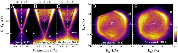
Fig.1 Fermi surface and band structure of Bi2Se3 cleaved in air and measured in the ultrahigh vacuum (UHV) chamber. (A) Band structure of the fresh Bi2Se3 cleaved and measured in the UHV chamber at 30 K along Γ−M direction. (B) Band structure of Bi2 Se3 cleaved in air and measured in UHV at 30 K along Γ−M direction. (C) Band structure of Bi2 Se3 cleaved in air and measured in UHV at 300 K along Γ-M direction.
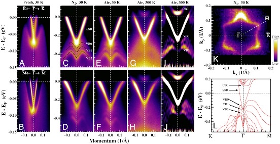
Fig.2 Persistence of topological surface state and formation of quantum well states in Bi2Te3 after exposure to N2 or air. The sample was first cleaved and measured in UHV at 30 K. (A and B) The corresponding band structure along the Γ-K and Γ-M directions. The sample was then pulled out from the UHV chamber and exposed to N2 at 1 atm for 5 min before transferring back into UHV chamber for the ARPES measurement. (C and D) The band structure of the N2-exposed sample along the Γ-K and Γ-M directions. The black dashed lines in C illustrate the quantum well states formed in the bulk valence band below the Dirac point. The sample was then pulled out again and exposed to air for 5 min before putting back in vacuum for ARPES measurement. (E and F) The band structure of the air-exposed sample at 30 K along the Γ-K and Γ-M directions. (G and H) The measurements at 300 K, and I and J show their corresponding second-derivative images in order to highlight the bands. (K) Fermi surface of N2-exposed sample. (L) First principle calculation of the band structure of Bi2Te3 slab with seven quintuple layers.
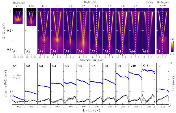
Fig.3 Evolution of surface state band structure and electron self-energy with the composition, x, in Bi2Te3−xSex system. (A) The surface state band structure of Bi2Te3−xSex with various compositions, x, measured along the Γ-K direction. (B) The surface state band structure of n- type Bi2Te3 along the Γ-K direction. (C) Corresponding effective real part of the electron self energy (black circles) and imaginary part of the electron self-energy (blue squares) for Bi2Te3−xSex with different compositions. (D) Corresponding effective real part of the electron self energy (black circles) and imaginary part of the electron self-energy (blue squares) for n-type Bi2Te3.
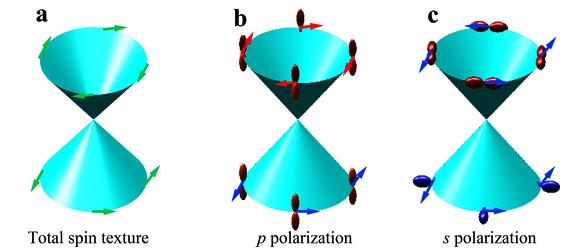
Fig. 4 Orbital textures probed in different polarization geometries and their coupled spin textures predicted for Bi2Se3 by theories. a. Schematic of the total spin texture for the surface Dirac cone of topological insulators. The arrows indicate spin directions. b. The pz orbitals selectively probed in the p polarization geometry and their expected spin texture. In this geometry, from the analysis of the photoemission matrix element effect, the ARPES signal is dominated by the out-of-plane pz orbitals for both the upper Dirac cone and the lower Dirac cone. It is expected that the pz orbitals are associated with a left-handed helical spin texture for the upper Dirac cone and a right-handed spin texture for the lower Dirac cone. c. Orbital textures probed in the s polarization geometry and their related spin textures. In this geometry, the ARPES signal is dominated by the in-plane tangential orbital texture for the upper Dirac cone and the in-plane radial orbital texture for the lower Dirac cone. It is expected that the tangential orbital texture in the upper Dirac cone is associated with a right-handed helical spin texture while the radial orbital texture in the lower Dirac cone is associated with a right-handed spin texture.
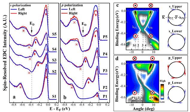
Fig. 5 SARPES measurements of the Bi2Se3 topological insulator under different light polarization geometries. a. Spin-resolved EDCs of the Bi2Se3 topological insulator at five representative momenta along the Γ-K momentum cut under the s polarization geometry. The spin-resolved EDCs are measured by the left (blue lines) and right (red lines) channels; each pair of the EDCs detects the in-plane spin component along the vertical z direction for a given momentum point. The corresponding momentum points are marked as the dashed lines in the band image measured from regular ARPES in the s polarization geometry(c). The EDC peaks corresponding to the bulk band, the upper Dirac cone and the lower Dirac cone are marked by empty circle, solid diamond and asterisk, respectively. b. Spin-resolved EDCs at five representative momenta along the Γ-K momentum cut in the p polarization geometry. The corresponding momentum points are marked as the dashed lines in the band image measured from regular ARPES in the p polarization geometry (d). On the right side of c, the measured spin texture measured in the s polarization geometry is shown for both the upper Dirac cone and the lower Dirac cone. On the right side of d, the measured spin textures measured in the p polarization geometry are shown.
Reference
[1] Fu, L., Kane, C. L. and Mele, E. J. Topological Insulators in Three Dimensions. Phys. Rev.Lett. 98, 106803 (2007).
[2] Qi, X.-L. and Zhang, S.-C. The quantum spin Hall effect and topological insulators. Phys.Today 63, 33 (2010).
[3] Hasan, M. and Kane, C. Colloquium: Topological insulators. Rev. Mod. Phys. 82, 3045 (2010).
[4] Zhang, H. Topological insulators in Bi2Te3, Bi2Te3 and Sb2Te3 with a single Dirac cone on the surface. Nat. Phys. 5, 438 (2009).
[5] Chen, C. et al. Robustness of topological order and formation of quantum well states in topological insulators exposed to ambient environment. Proceedings of the National Academy of Sciences 109, 3694 (2012).
[6] Guodong Liu, et al., Review of Scientific Instruments 79 (2008) 023105.
[7] Zhuojin Xie, et al. "Orbital-Selective Spin Texture and its Manipulation in a Topological Insulator" arXiv:1303.0698.
[8] Chen, C.Y. et al. Tunable Dirac Fermion Dynamics in Topological Insulators. Sci. Rep. 3, 2411; DOI:10.1038/srep02411 (2013)